Sporting Nations Project San Marino

We have now completed our contribution to the Sporting Nations Project initiated by The Embroiderers' Guild. Each branch was given a country and ours was San Marino, a small republic surrounded by Italy.
The embroideries below show our members interpretation of the geography and culture of that country carried out in a whole range of different stitch techniques. Our members should be very pleased with the colourful and attractive outcome.
The postcards will now be posted to Embroiderers' Guild house where they will be joined by all the other postcards from groups across Great Britain to be displayed at venues up and down the country in readiness for the Sporting Games.
Well Done and Thank You Everyone!


Posted in |

January Meeting 2012 Thread Bins

This month's meeting was led by one of our own members Anne Covell who showed us how to make Thread Bins for all our snippets of thread. The design was rather ingenious in that it telescoped down to a small flat cirle when folded away.


Anne showed us a completed bin and some half finished ones so that she could demonstrate how they were made and how the stitching joined the pieces together.


We made a tube of fabric and then cut out 2 x card circles, 2 x wadding circles and 2 x fabric circles larger than the card circles.
The fabric circles were gathered and pulled tightly over the card and wadding. This was done twice for the base and then the two separate pieces were sewn together.


A four inch inner tambour ring was slipped inside the half folded tube and stabbed stitched tightly in place.


The circles were then stitched in place one to one side of the doubled fabric one to the other. This was hard to imagine but Anne demonstrated on her half completed bins and it started to make sense.


At the end of the day we had all completed a thread bin something which happens very rarely as we usually run out of time. A big thank you to Anne for helping us make something attractive and also useful.


We will now be the neatest sewers around with all threads in our bins!!!


Posted in |

reticule

are more well-used in people's life. The reticule in wholesale city are so lovely that many girls fascinated with them. Let alone the cute appearance. They are the just right containers in most users' minds despite the small capacity. Their metal belts can be put into the handbags or taken off directly when you want to hold them. However, office females or those busy ones would prefer to the pocket-insidelarge reticule  are also very convenient for you to take the notebooks, files, books, cosmetics and other things. Thanks to those large handbags, holders look serious and easy-going, and they always match to the clothes you wear.

Handbags Elite

reticle

A reticle (or reticule) is a net of fine lines or fibers in the eyepiece of a sighting device, such as a telescope, a telescopic sight, a microscope, or the screen of an oscilloscope. The word reticle comes from the Latin "reticulum," meaning "net." Today, engraved lines or embedded fibers may be replaced by a computer-generated image superimposed on a screen or eyepiece. The term graticule is the synonymous term from French, it comes from the Latin craticula for gridiron. Both may be used to describe any set of lines used for optical measurement, but in modern use the term reticle is most commonly used for gunsights and such, while graticule is more widely used for the covers of oscilloscopes and similar roles.
There are many variations of reticles; this article concerns itself mainly with a simple reticle: crosshairs. Crosshairs are most commonly represented as intersecting lines in the shape of a cross, "+", though many variations exist, including dots, posts, circles, scales, chevrons, or a combination of these. Most commonly associated with telescopic sights for aiming firearms, crosshairs are also common in optical instruments used for astronomy and surveying, and are also popular in graphical user interfaces as a precision pointer. The reticle is said to have been invented by Robert Hooke, and dates to the 17th century.[1]

reticules

"All young ladies accomplished! My dear Charles, what do you mean?"
"Yes, all of them, I think. They all paint tables, cover screens, and net purses. I scarcely know anyone who cannot do all this, and I am sure I never heard of a young lady spoken of for the first time, without being informed that she was very accomplished.
Pride and Prejudice, chapter 8

Because the straight lines of Regency gowns did not provide room for pockets, women were forced to carry necessary items in small drawstring bags called reticules. Precursor to today's purse, the reticule provided a place to store important things (small parcels, spare change, the ever-present handkerchief, a small mirror, perhaps a snuffbox [all the rage at the time] or powder, smelling salts, and a love-letter or two) close at hand.

Reticules could be made of fabric coordinating with a particular gown or ensemble; some had papier mache bases and fabric tops. Toward the end of the Regency, they began using clasps as an alternative to the drawstring. Reticules frequently featured beading or embroidery and could be quite elaborate.

One other type of purse that was popular, was the "Miser's" or "Stocking" purse. Shaped like a tube (or sock) it had an opening in the center. When held in the middle you had two pockets in which to hold spare change. Rings slid down from the center to keep each side closed. Making purses was a popular pastime, as they could be knitted, netted or crocheted.


Visit the Boutique for a custom made Reticule

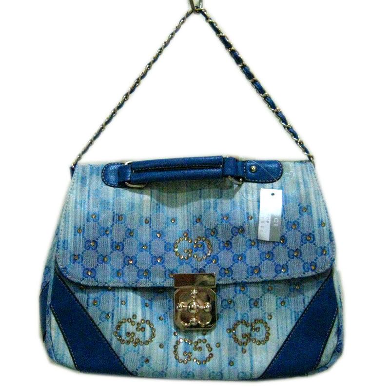
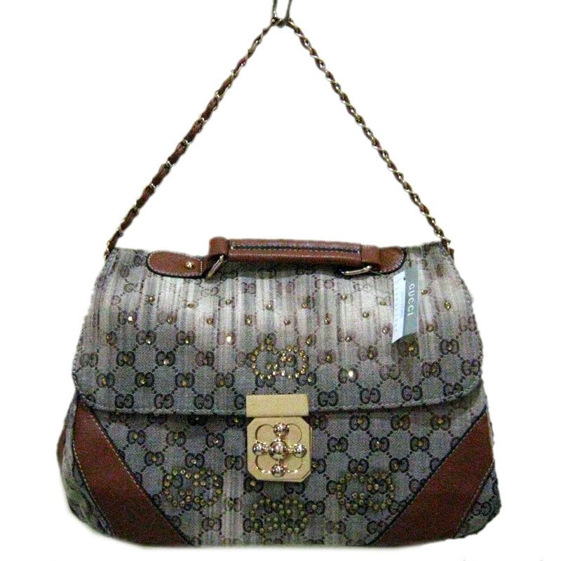
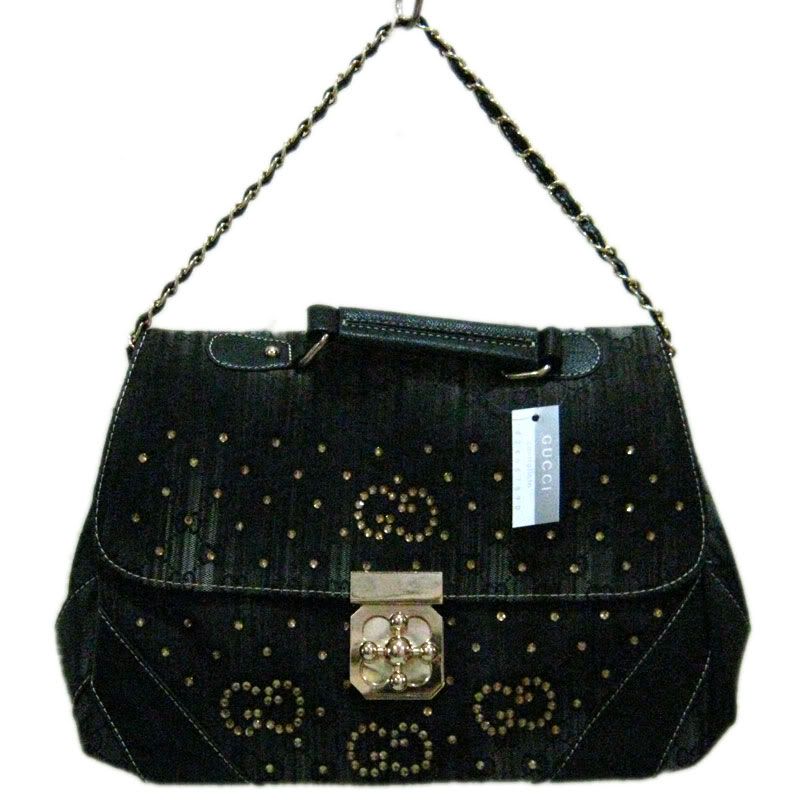
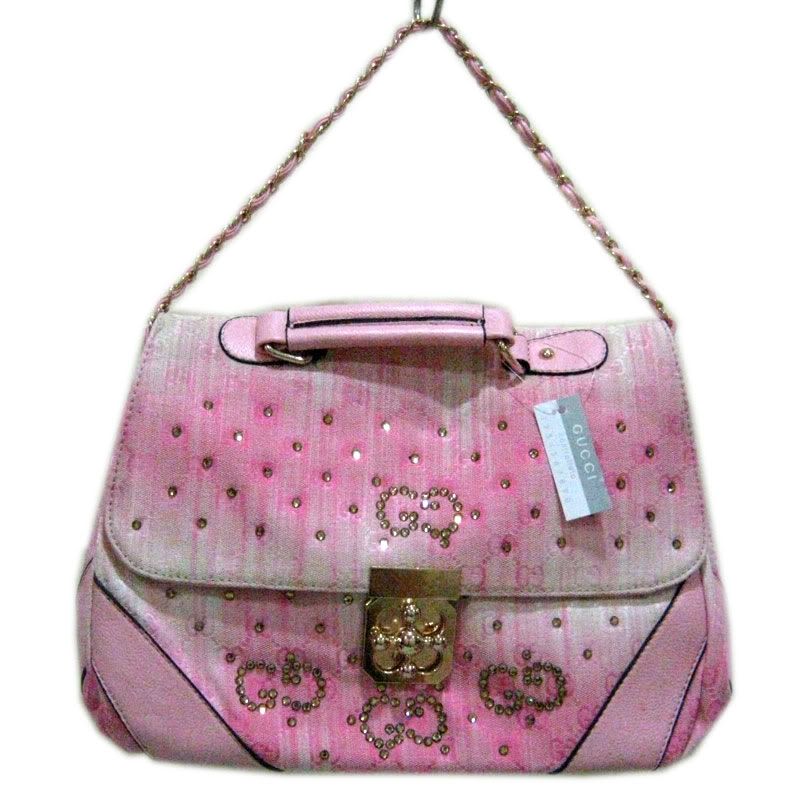
Tas Gucci 908

Tas Gucci 908

Tas Gucci 908-Biru Tas Gucci 908-Coklat Tas Gucci 908-Hitam Tas Gucci 908-Pink
(klik foto untuk memperbesar)
Kode Produk: Tas Gucci 908 (KW 1)
Warna: Biru, Coklat, Hitam, Pink
Dimensi: 32 x 25 x 11 (panjang x tinggi x tebal)
Info: Bahan kanvas mix kulit sintetis, ada sertifikat
Harga: Rp. 295.000

reticule definition

Photomask

From Wikipedia, the free encyclopedia
A photomask.
A schematic illustration of a photomask (top) and an integrated circuit created using that mask (bottom).
A photomask is an opaque plate with holes or transparencies that allow light to shine through in a defined pattern. They are commonly used in photolithography.

Contents

Overview

An actual photomask. The thicker features are the integrated circuit which is desired to be printed on the wafer. The thinner features are assists which do not print themselves but help the integrated circuit print better out-of-focus. The zig-zag appearance of the photomask is because optical proximity correction was applied to it to make it print better.
Lithographic photomasks are typically transparent fused silica blanks covered with a pattern defined with a chrome metal absorbing film. Photomasks are used at wavelengths of 365 nm, 248 nm, and 193 nm. Photomasks have also been developed for other forms of radiation such as 157 nm, 13.5 nm (EUV), X-ray and electrons and ions, but these require entirely new materials for the substrate and the pattern film.
A set of photomasks, each defining a pattern layer in integrated circuit fabrication, is fed into a photolithography stepper or scanner and individually selected for exposure. In double patterning techniques, a photomask would correspond to a subset of the layer pattern.
In photolithography for the mass production of integrated circuit devices, the more correct term is usually photoreticle or simply reticle. In the case of a photomask, there is a one-to-one correspondence between the mask pattern and the wafer pattern. This was the standard for the 1:1 mask aligners that were succeeded by steppers and scanners with reduction optics. As used in steppers and scanners, the reticle commonly contains only one layer of the chip. (However, some photolithography fabs utilize reticles with more than one layer patterned onto the same mask). The pattern is projected and shrunk by four or five times onto the wafer surface. To achieve complete wafer coverage, the wafer is repeatedly 'stepped' from position to position under the optical column until full exposure is achieved.
Features 150 nm or below in size generally require phase-shifting to enhance the image quality to acceptable values. This can be achieved in many ways, but the two most common methods are to use an attenuated phase-shifting background film on the mask to increase the contrast of small intensity peaks, or to etch the exposed quartz so that the edge between the etched and unetched areas can be used to image nearly zero intensity. In the second case, unwanted edges would need to be trimmed out with another exposure. The former method is attenuated phase-shifting, and is often considered a weak enhancement, requiring special illumination for the most enhancement, while the latter method is known as alternating-aperture phase-shifting, and is the most popular strong enhancement technique.
As leading-edge semiconductor features shrink, photomask features which are 4× larger must inevitably shrink as well. This could pose challenges as the absorber film will need to become thinner, and hence less opaque.[1] A recent study by IMEC has found that thinner absorbers degrade image contrast and hence contribute to line-edge roughness, using state-of-the-art photolithography tools.[2] One possibility is to eliminate absorbers altogether and use 'chromeless' masks, relying solely on phase-shifting for imaging.
The emergence of immersion lithography has a strong impact on photomask requirements. The commonly used attenuated phase-shifting mask is more sensitive to the higher incidence angles applied in "hyper-NA" lithography, due to the longer optical path through the patterned film.[3]

Mask Error Enhancement Factor

Leading edge photomasks contain (pre-corrected) images of the final chip patterns magnified by 4x. This magnification factor has been a key benefit in reducing pattern sensitivity to imaging errors. However, as features continue to shrink, two trends come into play: 1) the mask error factor begins to exceed 1, i.e., the dimension error on the wafer may be more than 1/4 the dimension error on the mask,[4] and 2) the mask feature is becoming smaller, and the dimension tolerance is approaching a few nanometers. As an example, a 25 nm wafer pattern should correspond to a 100 nm mask pattern, but the wafer tolerance could be 1.25 nm (5% spec) which translates into 5 nm on the photomask. The variation of electron beam scattering in directly writing the photomask pattern can easily well exceed this.[

Search

Swedish Greys - a WordPress theme from Nordic Themepark. Converted by LiteThemes.com.